
Before talking about the pros and cons, let’s clear out what Accelerated Mobile Pages actually means in terms of email marketing.
AMP for email was announced by Google back in 2018. It was presented as a new technology capable of giving an email to the functionality of the app. A wide audience of marketers got access to it in 2019, and since December 2019, the technology is supported for mobiles. This means now there are no reasons you can take advantage of the new functionality and spruce up your email campaigns. Or are there? Let’s take a look at why you need to consider including AMP in your email design arsenal, and what challenges to expect when doing so.
Main Advantages of AMP for Email
Novelty
Visual representation of emails hasn’t changed for a while. Yes, there were major technical updates, and trends in terms of layout design, but the way we see them in our inboxes remains pretty the same as 5 years ago. AMP can make a difference. It allows to make the outlook more dynamic, and content – more interactive, raising read time and engagement.
Moreover, it helps diversify your messages what can be essential if you regularly send 3-5 emails per week. We’re all get tired of monotony, and AMP-supported elements can add some contrast.
Wide functionality
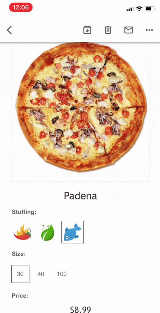
As for now, the AMP technology allows recipients to perform in emails the following:
- RSVP to an event (make an appointment, register for a webinar, make any booking, etc.);
- view a product catalog;
- leave a comment, review or feedback;
- make an order;
- fill in a survey or questionnaire.
All this can be done within the email body, and the recipient doesn’t have to open new windows and switch between tabs to complete a single action. It contributes greatly to shopping convenience, making the interaction with your brand more satisfying. And a satisfied customer has more chances to turn into a repeat and loyal one.
Additionally, such functionality helps not lose customers while they’re moving from email to website. Now, an email serves to both drive the attention to the product and encourage order completion.
Real-time updates of product information
AMP allows update product details (available colors and sizes, expired sales) in real time. It’s important because emails aren’t always opened right after delivery. But with AMP, whenever the subscriber opens your messages, it would contain only up-to-date information – available booking options, in stock, recent comments, etc.
If some offers have already expired (hot offers) by the moment the person reads the messages, they would know it. You’ll avoid those confusing situations when people respond to no longer active offers and listen to your apologies for providing irrelevant information.
Improved navigation
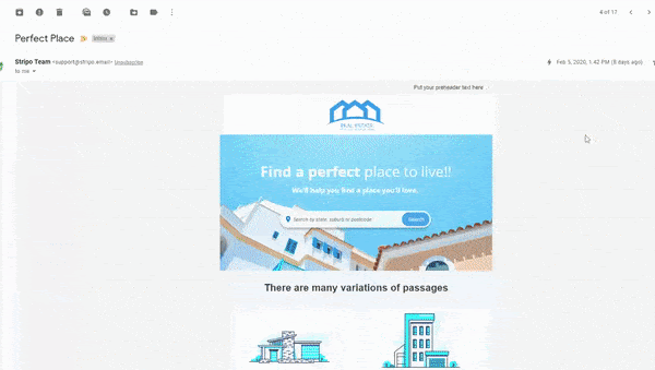
Such blocks as AMP accordion and carousel let give more information in less space, reducing the email length. The recipient doesn’t have to scroll through much which means they are less likely to miss out on significant information.
What’s more, such information can be rolled and unrolled, so the user choose themselves what part to see in details. The information that is currently irrelevant is hidden and doesn’t steal the attention. In a way, AMP contributes to content personalization as people can opt for what they’re most interested at the moment.
Ready AMP blocks
Most professional email service providers have long announced support of AMP and started developing the corresponding blocks for their editors. Depending on the platform, you can use such blocks as carousel, accordion, form, and feedback without code knowledge by simply dragging them to your template.
This is especially convenient for small companies without developer teams on their side. A regular marketer can use the technology by following instructions and simply filling the blocks with the necessary content. And with new blocks being added, your design arsenal will grow as well.
Main Disadvantages
There is no technology without cons, and AMP is no exception. Although I believe advantages outweigh the downsides, you need to know about possible issues you may face while working with AMP.
Not all email clients support it
By now, AMP for email is supported by Gmail, Outlook and Mail.ru. Yahoo has also announced support but it’s still in progress. When you send AMP messages to email clients that don’t support the technology, make sure they contain HTML duplicates so that all of your audience could see it.
Also, note that AMP emails may look different depending on the device and email client. Test emails before launching the campaign and make sure they’re optimized for desktop and mobile.
Not enough cases
Since the technology is relatively new and is only making its way into digital marketing, there aren’t many stats and cases available on AMP. Therefore, it’s impossible to learn from others, run competitive analysis, and see how the technology performs for your particular business. Plus, there is minimum material on AMP designs and usage tips. If you don’t want to use ready blocks and want custom solutions, you’ll have to learn the AMP code and build the design on your own.
Required registration with Google
I wouldn’t call it a disadvantage, rather a thing to keep in mind. To send AMP content, you need to be whitelisted by Google as a dynamic sender. You have to comply with the requirements (sender reputation, domain authentication), prepare two test emails (AMP/HTML), and fill in the application form. Approval can take up to two weeks, so if you plan to send AMP emails, it’s better to register in advance.
Like any other technology, AMP for email has its pros and cons. However, when used properly, it can bring you numerous advantages such as content diversity, deeper customer engagement, brand recognition, increase click rate, and ROI.